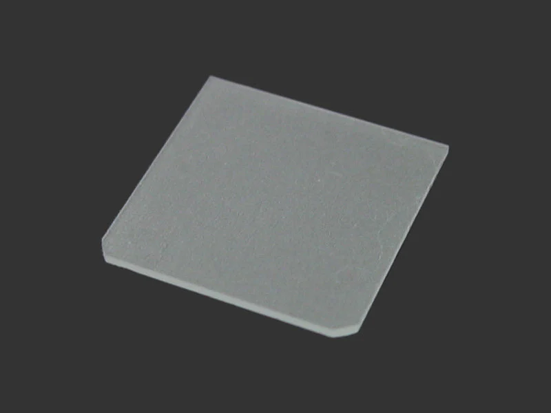

InP-(LEC- Grown) (100) S doped, 2"x 2.0 mm wafer, 1sp
InP single crystal wafer
Growing Method: LEC
Orientation: (100)
Size: 2" diameter x 2.0 mm
Doping: S- doped
Conducting type: N
Polish: one side polished
Resistivity: (1.1x10^-3 ohm.cm
Mobility: 1530 cmE2/V.S
EPD: <1.1x10^4 /cmE2
Carrier Concerntration: 3.6 x10^18 /cm^3
Ra(Average Roughness) : < 0.4 nm
Orientation: (100)
Size: 2" diameter x 2.0 mm
Doping: S- doped
Conducting type: N
Polish: one side polished
Resistivity: (1.1x10^-3 ohm.cm
Mobility: 1530 cmE2/V.S
EPD: <1.1x10^4 /cmE2
Carrier Concerntration: 3.6 x10^18 /cm^3
Ra(Average Roughness) : < 0.4 nm


$803.25
Original: $2,295.00
-65%InP-(LEC- Grown) (100) S doped, 2"x 2.0 mm wafer, 1sp—
$2,295.00
$803.25Product Information
Product Information
Shipping & Returns
Shipping & Returns
Description
InP single crystal wafer
Growing Method: LEC
Orientation: (100)
Size: 2" diameter x 2.0 mm
Doping: S- doped
Conducting type: N
Polish: one side polished
Resistivity: (1.1x10^-3 ohm.cm
Mobility: 1530 cmE2/V.S
EPD: <1.1x10^4 /cmE2
Carrier Concerntration: 3.6 x10^18 /cm^3
Ra(Average Roughness) : < 0.4 nm
Orientation: (100)
Size: 2" diameter x 2.0 mm
Doping: S- doped
Conducting type: N
Polish: one side polished
Resistivity: (1.1x10^-3 ohm.cm
Mobility: 1530 cmE2/V.S
EPD: <1.1x10^4 /cmE2
Carrier Concerntration: 3.6 x10^18 /cm^3
Ra(Average Roughness) : < 0.4 nm