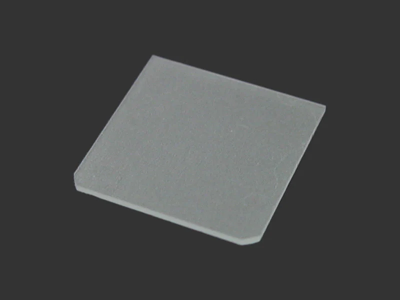

Ge Wafer (110) 2" dia x 0.8 mm, Fine ground , N type ( Sb doped), resistivities: 0.1-0.5 ohm-cm
Ge Wafer Specification
-
Growing Method: CZ
-
Orientation: (110)
-
Wafer Size: 2" dia x 0.8mm
-
Surface Polishing: Fine ground
-
Doping: Sb Doped
-
Conductor type: N-type
-
Resistivity: 0.1-0.5Ohm.cm (If you would like to measure the resistivity accurately,
please order our Portable 4 Probe Resistivity Testing Instrument.)
Typical Properties:
- Structure: Cubic, a = 5.6754 A
- Density: 5.323 g/cm3 at room temperature
- Melting Point: 937.4 oC
- Thermal Conductivity: 640
Related Product
|
|
|
|
|
|
|
Other Crystal wafer A-Z |
Plasma Cleaner |
Wafer Containers |
Dicing saw |
Film Coater |


$125.65
Original: $359.00
-65%Ge Wafer (110) 2" dia x 0.8 mm, Fine ground , N type ( Sb doped), resistivities: 0.1-0.5 ohm-cm—
$359.00
$125.65Product Information
Product Information
Shipping & Returns
Shipping & Returns
Description
Ge Wafer Specification
-
Growing Method: CZ
-
Orientation: (110)
-
Wafer Size: 2" dia x 0.8mm
-
Surface Polishing: Fine ground
-
Doping: Sb Doped
-
Conductor type: N-type
-
Resistivity: 0.1-0.5Ohm.cm (If you would like to measure the resistivity accurately,
please order our Portable 4 Probe Resistivity Testing Instrument.)
Typical Properties:
- Structure: Cubic, a = 5.6754 A
- Density: 5.323 g/cm3 at room temperature
- Melting Point: 937.4 oC
- Thermal Conductivity: 640
Related Product
|
|
|
|
|
|
|
Other Crystal wafer A-Z |
Plasma Cleaner |
Wafer Containers |
Dicing saw |
Film Coater |