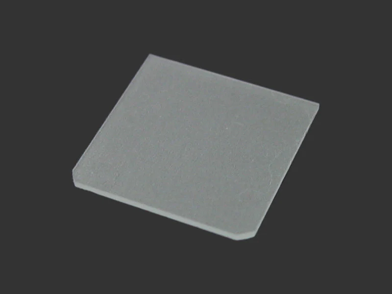

GaN Template on Sapphire(11-02) , 5 x 5 mm x 0.5mm ,1sp, GaN film: 5um - FmGaNonALR050505S1FT5um
GaN Template on saphhire is made by a hydride vapor phase epitaxy (HVPE)-based method. During the HVPE process, HCl reacts with molten Ga to form GaCl, which in turn reacts with NH3 to form GaN. GaN template is a cost effective way to replace GaN single crystal substrate
Specifications
- Sizes 5mmx5mm
- Substrate Sapphire, Orientation R (00.1) +/- 1.0 o
- Conduction Type: n-type,
- Resistivity < 0.5 Ohm-cm
- Front Surface Finish (Ga Face) As-grown
- Back Surface Finish Sapphire as-received finish
- Useable Surface Area >90%
- Edge Exclusion Area 1mm
- Package Single Wafer Container
- GaN layer thickness 5 microns , (=/- 10%)
- Please click here to see XRD Rocking curve of GaN template
- Please click here to see Dislocation vs Thickness of GaN template
- Please click here to see RMS of GaN template
Related Products
 |
|
|
|
|
|
Thin Films A-Z |
Crystal wafer A-Z |
Plasma Cleaner |
Wafer Containers |
Dicing saw |
Film Coater |


Product Information
Product Information
Shipping & Returns
Shipping & Returns
Description
GaN Template on saphhire is made by a hydride vapor phase epitaxy (HVPE)-based method. During the HVPE process, HCl reacts with molten Ga to form GaCl, which in turn reacts with NH3 to form GaN. GaN template is a cost effective way to replace GaN single crystal substrate
Specifications
- Sizes 5mmx5mm
- Substrate Sapphire, Orientation R (00.1) +/- 1.0 o
- Conduction Type: n-type,
- Resistivity < 0.5 Ohm-cm
- Front Surface Finish (Ga Face) As-grown
- Back Surface Finish Sapphire as-received finish
- Useable Surface Area >90%
- Edge Exclusion Area 1mm
- Package Single Wafer Container
- GaN layer thickness 5 microns , (=/- 10%)
- Please click here to see XRD Rocking curve of GaN template
- Please click here to see Dislocation vs Thickness of GaN template
- Please click here to see RMS of GaN template
Related Products
|
|
|
|
|
|
Thin Films A-Z |
Crystal wafer A-Z |
Plasma Cleaner |
Wafer Containers |
Dicing saw |
Film Coater |